THE CHALLENGE
Current electronic devices are limited by electron transport speed. Due to the limits of their materials, conventional electronics allow only diffusive electron transport motion and only in one dimension. Advances in material purity are allowing newly discovered ballistic and hydrodynamic electron transport regimes to be reached in solid state materials, resulting in more useful current-voltage characteristics than in current silicon devices.
Exploiting these advantages can lead to next-generation devices capable of high-frequency, low-noise, low heat dissipation, and low power-consumption operation.
OUR SOLUTION
Devices that enable ballistic-hydrodynamic electron transport achieve considerable advantages over existing technology. This technology offers gallium arsenide/aluminum gallium arsenide (GaAs/AlGaAs) heterostructures that leverage advanced materials purity and device design to achieve non-diffusive ballistic and hydrodynamic electron transport regimes in two-dimensional electron systems. These devices are inherently non-linear and have high electron mobility at low temperatures, which allows configuration as switches or amplifiers that can operate in micrometer and millimeter wave applications.
GaAs/AlGaAs devices use well-established fabrication techniques yet offer nonlinear and nonlocal current-voltage characteristics and enable features that are not possible with the diffusive transport characteristics of conventional electronics.
These devices are expected to outperform standard silicon and III-V semiconductor products, a result stemming from the efficiency of the electron transport systems and enabling of new functionalities. Additionally, the manufacturing process is simplified compared to existing and next-generation devices. A new generation of products is possible that is capable of higher frequency operation (in the microwave or millimeter wave regimes), inherently lower heat dissipation, and lower power consumption.
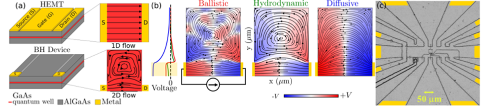
Figure: Schematics of the technology involved: a) Comparison of a conventional transistor with 1D flow vs. ballistic-hydrodynamic device with 2D flow; b) flow profiles obtainable in different electron transport regimes; and c) micrograph of a fabricated device showing the small, central square as the active area.
Advantages
- Faster: Device design and materials enable ballistic transport resulting in faster switching and higher frequency operation.
- Higher performance: System creates significantly less heat and power dissipation, and consumes less power, combining to achieve better device performance.
- Efficient: Simplification of the fabrication process, along with improved performance features, leads to higher efficiency electronic devices.
Potential Applications:
- High frequency applications, such as:
- Signal mixers
- Frequency multipliers (upconverters)
- Frequency downconverters
- Rectifiers
- Signal detectors
- Transconductance amplifiers
- Telecommunications systems
- Radar systems
- Low-noise, high-speed interface electronics for quantum information technologies and neuromorphic logic
- Detection circuitry in highly sensitive astrophysical observation equipment